
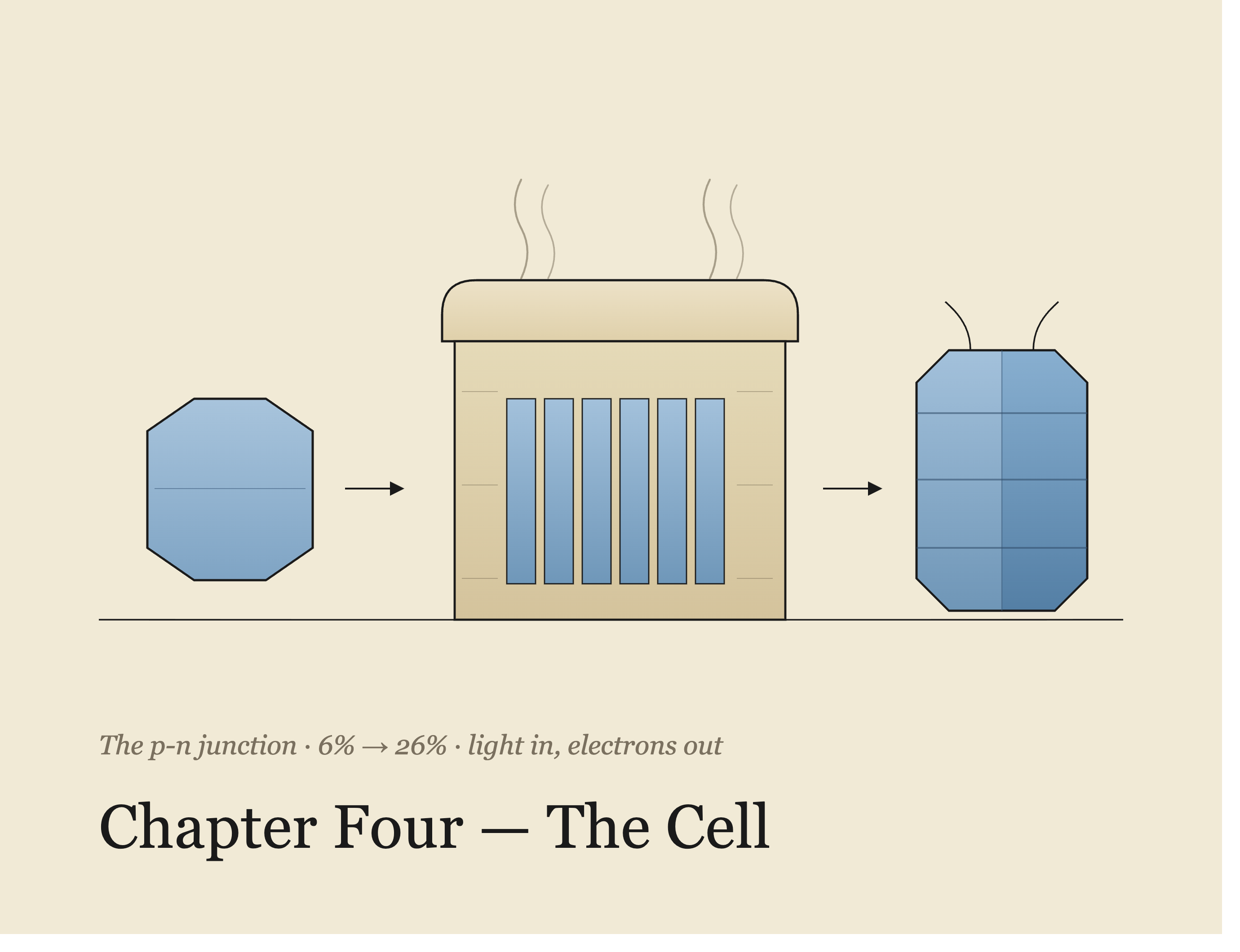
The Solar Value Chain Decoded · Chapter Four
The Cell

An eight-part field guide to the people, places, and machines that stand between a vein of rock and the panel on your roof. In the first three chapters we dug the quartz out of an Appalachian valley, refined it in billion-dollar reactors into hyper-pure silicon, and grew that silicon into a single perfect crystal which we then sliced, thinner than paper, into wafers. Now the wafer, that flawless blank, finally learns to do something.
At the end of the last chapter I left you with a stack of solar wafers: paper-thin, mirror-flat, brittle squares of pure crystalline silicon, each of them a small marvel of manufacturing patience. Every atom sits where it should. There are no crystal boundaries, no impurities of any consequence, no waste. The silicon has been through a rock crusher, a submerged-arc furnace, a chlorine bath, a distillation column, a 1,400-degree crucible of Spruce Pine quartz, and finally a diamond wire. And after all of that, the wafer cannot do a single useful thing.
You could lay one on the roof of your house on the sunniest day of the year and it would sit there, warm, and produce nothing at all. Zero volts. Zero amps. Zero watts.
I want you to sit with that for a moment, because it is the punchline of the previous three chapters, and it points at what this one is really about. The staggering effort we have just watched — the mine, the refinery, the crystal — was not, as it might have seemed, the effort of making electricity from sunlight. It was the effort of preparing the material to begin being able to do that. Everything up to now has been buildup. This chapter is where the wafer, at last, becomes a machine.
And the astonishing part is how little you have to do to it. The chemistry that separates a useless slab of silicon from a device that turns roughly a quarter of the sunlight falling on it into electricity is, in the physical sense, almost trivial. A handful of atoms in the right places. A whisper of another element. That is the whole trick.
It is also the trick that has been costing a great many people a great many billions of dollars to get right by the smallest possible margins, for the last seventy years.
The trick discovered by a teenager
Let me begin, as this series has now got into the habit of doing, with the fact that made the whole thing possible in the first place, and with the person who found it.
The year is 1839, and a nineteen-year-old French physics student named Edmond Becquerel is working in his father's laboratory in Paris. He is playing with electrodes and electrolyte solutions, running experiments the way a certain kind of young man plays a musical instrument. In the course of one particular setup, he notices something odd: when he shines light on one of the electrodes immersed in the solution, a small electric current appears where there was none before. Cover it up, the current stops. Uncover it, the current returns. He writes it up in a short paper. He is, at that moment, the first human being to observe what we now call the photovoltaic effect — the direct conversion of light into electricity — and he is, at that moment, nineteen years old.
For the next hundred and fifteen years, essentially nothing happens with it. Becquerel's observation is a curiosity, and it stays a curiosity. The effect appears in every physics textbook of the nineteenth century in the way a talented but obscure musician is admired by a small circle and ignored by everyone else. Nobody builds anything with it, because nobody understands why it happens, and the currents are too small to be of any practical use.
The reason nobody built anything with it for over a century is that the effect only becomes engineeringly useful when you know one particular thing about silicon — a thing that was, in 1839, still eighty years from being discovered. What Becquerel had glimpsed is that light, when it strikes certain materials, can knock electrons free of their atoms. That much is easy to state. The subtler part is this: knocking an electron loose is only half of a solar cell. If the electron simply pops out of place and then falls back in a moment later, no current flows. You need to persuade the electron to go somewhere useful — to travel in a single, predetermined direction, through an external circuit, and do work — before it settles back down. And to do that, you need to build a road with a one-way sign on it, inside the silicon itself.
That is what the rest of this chapter is about.
The one-way street
Return to the wafer. It is 150 microns thick, mirror-smooth, chemically inert, and full of silicon atoms locked into a perfect lattice. The mobile electrons inside it — the ones that could, in principle, be dislodged by light — have no reason to go one way rather than another. Left to themselves, they slosh around at random. What you need to do, to make a solar cell, is impose a preferred direction on them without touching the perfect lattice you have gone to such trouble to grow.
The trick is called doping, and it is one of those industrial words that sounds vaguely disreputable and turns out to be almost supernaturally clever.
You take your pure silicon wafer, heat it in a furnace, and introduce — in vanishingly small quantities, a few atoms per million — a whiff of another element. Phosphorus, say. A phosphorus atom is almost the same size as a silicon atom, so it can slip into the crystal lattice without breaking anything; it takes a silicon atom's place as if nothing had happened. But a phosphorus atom has five outer electrons where silicon has four. Once it settles into the lattice, four of those electrons are used up bonding to the neighbors — and the fifth has nothing to do. It is a spare electron, loosely tethered, easily persuaded to wander. Do this to enough atoms across one face of the wafer, and you have created a region rich in spare, mobile electrons. We call this n-type silicon, for the negative charge those spare electrons carry.
Now do the mirror image on the other side. Introduce a whiff of boron instead of phosphorus. Boron has three outer electrons — one short of silicon. Where each boron atom sits in the lattice, there is a small hole, a missing electron, waiting to be filled. This is p-type silicon, for the positive charge the missing electron effectively represents.
You now have a wafer with a strange geography. One face is populated by spare electrons wanting to move; the other face is populated by missing electrons — call them holes — also wanting to move. And where the two regions meet, in a thin invisible zone inside the wafer only a fraction of a micron thick, an extraordinary thing happens. The spare electrons on the n-side, purely by diffusion, wander across the boundary into the p-side, where they fill the waiting holes. But as they cross, they leave behind, on the n-side, positively-charged phosphorus atoms; and as they arrive, on the p-side, they turn boron atoms into negatively-charged ions. Very quickly, an electric field builds up across the boundary: positive on the n-side, negative on the p-side. The field pushes back against any further electron migration, and equilibrium is reached.
That built-in electric field is the whole point. It is the one-way sign in the road. From now on, any electron dislodged by a photon anywhere in the neighborhood of the boundary will be shoved, involuntarily, toward the n-side. Any hole will be shoved toward the p-side. The wafer no longer has to decide what direction electrons should travel. Its own internal geometry decides for them.
This is a p-n junction, and it is the beating physical heart of every silicon solar cell ever made. Photograph a hundred cells from a hundred different manufacturers and, underneath the paint and the trim and the marketing acronyms, they all bottom out at the same phenomenon: two doped layers of silicon, meeting at a boundary a few tenths of a micron thick, holding a built-in electric field. Everything else in cell manufacturing — every subsequent process step, every generation of technology from PERC to TOPCon to heterojunction — is, at bottom, an attempt to get more photons in, get more electrons out, and lose fewer of them along the way.
Bell Labs, 1954: the first useful cell
The gap between Becquerel's teenage discovery in 1839 and a solar cell you could actually plug into something was closed, as most large gaps in twentieth-century technology were, in New Jersey. In April 1954, three researchers at Bell Labs — Daryl Chapin, Calvin Fuller, and Gerald Pearson — held a press conference to announce something the world had, in a low-grade way, been waiting a century for: a silicon solar cell that worked. It converted about 6 percent of the sunlight falling on it into usable electricity. That was a leap of an order of magnitude over anything that had come before, and it made the front page of the New York Times, which cheerfully declared the beginning of "a new era."
The new era did not, in fact, begin. The Bell cell was, by any reasonable industrial measure, catastrophically expensive: it cost several hundred dollars per watt in 1954 dollars, which for context is on the order of thousands in modern money. It was useful for exactly one application where cost per watt was almost irrelevant, and that application was the American space program. For the next twenty years, essentially every silicon solar cell in existence was bolted to the side of a satellite. The first was on Vanguard 1, launched in 1958, whose solar cells kept its radio pinging back to Earth for six years after its chemical batteries died. If you go and look up Vanguard 1 today, you will discover that it is still in orbit. It is the oldest human-made object in space. Its solar cells long ago faded out, but the little piece of doped silicon that Chapin, Fuller, and Pearson made possible is still up there, quietly circling the planet, a small metal witness to the beginning of an industry.
What has happened between 1954 and today is one of the most spectacular learning-curve stories in modern industry. A watt of solar cell that cost several hundred dollars in 1954 costs, in 2026, on the order of ten cents. That is a factor of several thousand, sustained over seventy years, across a technology whose basic physics has never really changed. It is a slower version of the story of computing — of Moore's law — with the crucial difference that solar's learning curve was not driven by making the feature smaller, but by making the process better. Every single one of those factor-of-two cost declines, and there have been many of them, was engineered by someone shaving a fraction of a percent off wafer thickness, or off silver usage, or off electrical loss at the contacts, or off reflection from the front surface. It is a story about caring, obsessively, for seven decades, about the parts of the cell most people would not think to look at.
Which brings us to the number the industry has, in fact, been obsessing over.
What a single percentage point is worth
Efficiency, in a solar cell, means one thing and one thing only: the fraction of the solar energy falling on the cell that leaves it as electrical energy. Everything else — the fill factor, the open-circuit voltage, the temperature coefficient — is engineering plumbing. What the customer buys, in the end, is the fraction.
That fraction has a hard ceiling, and it was proven mathematically in 1961 by two physicists, William Shockley and his young collaborator Hans-Joachim Queisser. What they showed is that for a single-junction solar cell — one wafer, one p-n junction — the maximum theoretical conversion efficiency, for an ideal material with a perfect bandgap, is around 33 percent. Silicon, whose bandgap is close to but not exactly optimal, comes in a little lower: something like 29 percent once you account for the ways in which real silicon, unlike ideal silicon, quietly leaks energy back as heat. Above that, the physics simply forbids it. Half the incoming sunlight is in photons whose wavelengths are wrong for silicon — too red to knock an electron loose, or too blue and mostly wasted as heat. The gap between "what light delivers" and "what silicon can absorb" is a mathematical wall.
In 1954, Bell Labs was at 6 percent. Commercial cells crawled to 10 percent by the 1980s, 15 percent by the early 2010s, 18 percent by mid-decade. Today, the best mass-market commercial cell hovers around 24 to 26 percent, with laboratory records inching just past 27. Which means we are, at last, within striking distance of the physical ceiling — perhaps two or three percentage points from what the universe permits.
To an outsider, this sounds like a small margin — and a slow-moving fight. Two points, over half a decade of R&D. Who cares?
Here is who cares. A one-percentage-point improvement in cell efficiency reduces, by roughly one percent, the number of cells you need to build to deliver a given quantity of power. Which reduces, by roughly one percent, the amount of glass, aluminum frame, encapsulant, backsheet, junction box, and labor that goes into each watt shipped. And it reduces, by roughly one percent, the area of land — or roof — that a given project needs to occupy. Multiply that by the several hundred gigawatts of solar being installed each year, and a single percentage point of cell efficiency is worth, over the life of the assets it goes into, tens of billions of dollars. This is why the world's largest cell manufacturers publish press releases every few weeks announcing world-record efficiencies to two decimal places. It is not vanity. Every hundredth of a percent is a real number, denominated in real dollars, distributed across a real portion of the world's electricity system.
And it is why, over the past three years, the entire cell industry — quietly, and almost invisibly to buyers — swapped out the recipe.
The workhorse: PERC
To understand the change, meet the recipe it replaced.
For most of the last decade, the dominant industrial cell design was called PERC — Passivated Emitter and Rear Cell. The name is dry; the idea is elegant. Take an ordinary p-type silicon wafer, do the doping we described earlier, and then add one crucial refinement: coat the back of the cell with a very thin passivation layer that reflects any photon that made it all the way through the silicon without being absorbed, sending it back for a second chance, while also chemically calming the back surface so that the electrons that reach it are not immediately lost to defects. That, in one sentence, is PERC. It looks like a modest tweak. In practice it lifted cell efficiencies by roughly a full percentage point across the industry, and for a number of years it was the closest thing solar had to an industry standard.
By the mid-2010s, virtually every major Chinese manufacturer — Longi, Trina, JinkoSolar, Canadian Solar, and dozens of others — was building PERC cells at enormous scale. It was the technology that took solar from being the expensive alternative to being, cell-for-cell, cheaper than any other form of new generation on the planet. If you have installed a solar panel between roughly 2016 and 2022, there is a very good chance it is PERC underneath.
But PERC has, or had, a ceiling. It is built on a p-type wafer, and p-type silicon carries a subtle limitation the industry took years to fully appreciate: it develops a specific kind of defect, called light-induced degradation, when exposed to sunlight for the first time. The industry learned to compensate for it, but it left roughly half a percentage point of efficiency permanently on the table. And the physical geometry of PERC — the way the metal contacts run across the front of the cell, blocking sunlight from a small but stubborn percentage of the surface — was becoming harder and harder to improve on. By the early 2020s, PERC had, essentially, run out of headroom.
So the industry did the thing industries almost never do voluntarily: it changed the wafer.
The quiet migration to TOPCon and HJT
Around 2023, and accelerating through 2024 and 2025, the leading manufacturers switched, at enormous cost, from p-type PERC to a family of n-type designs. The best-known of these is called TOPCon — Tunnel Oxide Passivated Contact — which uses an n-type wafer instead of a p-type, applies a much more sophisticated passivation stack to the back surface, and pushes cell efficiencies about one to one and a half percentage points above PERC. Alongside it, a smaller but faster-growing technology called heterojunction, or HJT, layers ultra-thin amorphous silicon films on top of a crystalline n-type wafer to squeeze another fraction of a percent out and, crucially, to perform much better at high temperatures — which matters, because a hot roof gives you less power than a cool one. Between them, TOPCon and HJT are now, in 2026, the recipe of essentially every high-performance panel arriving on an American commercial rooftop. The p-type era is over.
And here is the thing about that transition I keep returning to, because it is such a good illustration of how this industry actually works. The buyer of a pallet of solar modules in Georgia in 2026 is almost certainly buying TOPCon cells. In 2022 they would almost certainly have been buying PERC. Somewhere between those two dates, tens of billions of dollars of manufacturing capex were poured into rebuilding cell lines, and the recipe of every panel changed — and to the person specifying and installing them, the change was almost imperceptible. The panel looked the same. The datasheet was slightly different — a few more watts, a slightly better temperature coefficient, a marginally different voltage curve — but nothing that shouted "new technology." The buyer bought a solar panel. What they got was a completely re-engineered device with a fundamentally different physics underneath.
This is the pattern I want you to notice. In the mine, the drama was geological. In the refinery, geographical. In the wafer factory, industrial. In the cell factory, it is technological — and it moves fast. Not fast like software; there are no annual release cycles here, no over-the-air updates. But fast in the sense that the recipe of the thing you are buying can be quietly re-engineered underneath you in a single procurement season, and you can go on writing purchase orders as if nothing has changed while an entire industry rebuilds itself around you. The buyer who bought PERC in 2022 and TOPCon in 2024 probably did not notice — but the manufacturers behind them noticed. They spent, between them, something on the order of fifty billion dollars to make that changeover happen.
The lesson is not that you should worry about which specific letter of the alphabet is on the cell inside your module. It is that the technology in solar is now moving faster than the buying process is designed to track, and that the honest way to specify a panel is not by acronym but by outcome — efficiency, temperature coefficient, warranty, degradation curve. The acronym will change again in the next few years. What you actually care about — how much power you get, at what price, for how long — will not.
Where cells get made
If you are keeping the geographical scorecard for this series, the cell layer offers a slightly less concentrated map than the wafer, and for reasons worth understanding.
China still dominates cell manufacturing — by most counts producing three-quarters or more of the world's cells — but the concentration is meaningfully looser than in wafers, and it has been loosening further. Cell factories have, over the past decade, spread into Vietnam, Malaysia, Thailand, and Cambodia, which has for years been the workaround of choice for panels destined for the US market: Chinese wafers, cells made in Southeast Asia, modules assembled from those cells and shipped to America under a different origin. The recent tightening of US trade rules — antidumping and countervailing duty cases layered on top of the UFLPA — has made even that route more complicated, but it explains why so many of the panels the American market has been consuming come, on paper, from countries that had no meaningful solar industry a decade ago.
The United States has begun, tentatively, to build cell capacity of its own. Several plants are under construction or ramping up in Georgia, Texas, and Ohio, backed by the manufacturing tax credits of the Inflation Reduction Act. As with polysilicon refining and wafer growing, this exists because of policy rather than pure economics; without the credits, the electricity and labor costs would not pencil. But it is real, and it is the layer that, together with the wafer, will determine whether an American-made solar panel is one day possible in any meaningful sense of the phrase. Until there is significant US cell capacity, "made in America" for solar modules ends at the module frame.
What the cell teaches us
Step back once more, and note what has just happened to the story.
The mine taught us the chain is narrow. The refinery taught us it is concentrated and political. The wafer taught us it is deep in expertise. The cell adds one more property, and it is the one that matters most to the buyer: the chain is fast. The recipe of the device you are installing has been quietly rebuilt in the last three years. It will be rebuilt again, in a different way, before the decade is out. The manufacturers you buy from are running an efficiency race in which every hundredth of a percentage point is a bid for survival, and the winners are the ones who can pour billions into changing their process on a five-year cycle without ever raising a price by more than the market will bear.
There is a lesson buried in this for anyone specifying panels in America right now, and it is worth stating plainly, because it is one that quietly haunts every procurement decision in this industry.
The layer where technology moves fastest is not the layer where trade policy moves fastest. Cells improve every year. Regulations, tariffs, and tax-credit rules move on their own, largely uncoordinated schedule. This mismatch — between how quickly the physical product is getting better and how slowly the paperwork is catching up — is why the modern American solar buyer has to think about two things at once that used to be one. What is the right cell for my project, physically and economically? And what is the legal cell for my project, given where each of its layers was made? Those two questions used to have the same answer. Increasingly, they do not.
The next chapter is where those two questions finally collide, because the module — the panel itself, the thing with the frame and the glass and the junction box — is the layer where "made in" gets stamped. The cells go into the module factory. What comes out is a solar panel with a country of origin, a warranty, a nameplate wattage, and — depending on how it was assembled — an eligibility, or not, for the tax credits and domestic-content bonuses that shape the American market.
The module is where the value chain, at last, meets the commercial world. It is the first layer the buyer has ever actually seen.
This series is published by SolarStock USA. We distribute Sunpro Power modules from inventory positioned in the United States. We wrote this guide because we believe the people who buy, specify, and install solar deserve to understand the whole chain they are part of — not just the part that touches their invoice.