
The Solar Value Chain Decoded · Chapter Three
The Ingot & the Wafer

An eight-part field guide to the people, places, and machines that stand between a vein of rock and the panel on your roof. In the first two chapters we dug the quartz out of an Appalachian valley and refined it, in billion-dollar reactors, into chunks of hyper-pure silicon. Now comes the strangest transformation of all: turning a tray of grey beads into a single flawless crystal the length of your arm, and then slicing that crystal into wafers thinner than a sheet of paper — by the hundred million.
By the time silicon reaches the third layer of the chain, it has already had a remarkable life. It began as a rock in a mountain in North Carolina. It was crushed, refined, superheated, and reborn as polysilicon — chunks and rods and beads of grey, glassy material, refined to a purity that beggars the imagination. If you held a handful of it, it would look like nothing. Aquarium gravel, maybe, or the granules at the bottom of a very expensive bag of cement. It is, at this point, the purest mass-produced substance on Earth, and it is also completely useless.
That is the thing nobody tells you about polysilicon. Purity is necessary, but purity alone does not generate a single watt of electricity. You can have the cleanest silicon in the universe sitting in a barrel, and it will do absolutely nothing useful, because the atoms inside it are arranged at random — a chaotic jumble, each grain a tiny crystal pointing whichever way it cooled. To turn this into something that can catch sunlight and push electrons in a useful direction, you have to perform a kind of atomic choreography. You have to take all those randomly arranged atoms and persuade every single one of them to fall into line, into one continuous, perfect, repeating lattice, across a crystal the size of a fence post.
This chapter is about how that is done. It is the least visible step in the entire solar story — there are no mines to photograph, no Xinjiang controversy, no town of two thousand people. It happens inside sealed furnaces and behind the closed doors of a handful of factories, almost all of them in China. And yet it is, to my mind, the most quietly astonishing thing that happens to a solar panel on its whole journey from rock to roof. It is the moment the silicon stops being a material and starts becoming a machine.
The crystal grown from a single seed
Recall, from the first chapter, the catch that put a town in North Carolina at the center of the world: to make a good solar cell you need a near-perfect crystal, and to grow a near-perfect crystal you need to melt purified silicon in a crucible of Spruce Pine quartz. We can now watch that actually happen.
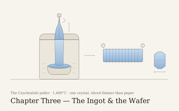
The dominant method is the one named after Jan Czochralski — the Polish chemist whose accidental discovery in 1916 we met in the first chapter. In its modern industrial form it is a marvel of patience disguised as a furnace. You load your polysilicon — those grey beads — into the quartz crucible, and you heat it past 1,400 degrees Celsius, hotter than flowing lava, until it becomes a pool of glowing, liquid silicon. Then, instead of pouring or stamping or casting it the way you would any other molten material, you do something almost delicate. You lower a single small "seed" crystal, no bigger than a pencil stub, until its tip just kisses the surface of the melt.
And then you pull.
Slowly — millimeters per minute — you draw the seed back upward, rotating it as you go, and the molten silicon clings to the seed and solidifies onto it. But here is the wonder of it: it does not solidify at random. It solidifies in the same crystal pattern as the seed. The seed is a template, a single perfect fragment of lattice, and as you pull it up out of the melt, atom by atom, the liquid silicon freezes onto it in lockstep, every atom snapping into the exact position the seed dictates. The crystal grows downward from the seed into a fat cylindrical column called an ingot — or, in the trade, a boule — sometimes two meters long and weighing several hundred kilograms, and the entire thing, from top to bottom, is one single crystal. One continuous, unbroken lattice. There is no other word for it but grown. It is closer to cultivating a pearl than to manufacturing a part.
The whole operation takes the better part of a day for a single ingot, and it has to be done in an atmosphere of inert argon gas, because oxygen would ruin everything, and it cannot really be hurried, because if you pull too fast the lattice stumbles and the crystal goes polycrystalline — back to the useless jumble — and the run is spoiled. A modern "puller," as the machines are called, is a tall steel cylinder two or three stories high, humming quietly in a row of identical siblings on a factory floor, each one slowly hauling a glowing rod of perfect silicon up out of a pool of liquid fire. It is one of the most beautiful processes in all of manufacturing, and almost nobody outside the industry has ever seen it.
There is an older, cheaper cousin to this method worth mentioning, because for years it was half the market. Instead of pulling a single crystal, you can simply pour molten silicon into a large square mould and let it cool slowly, producing a block in which the silicon has crystallized into many crystals fused together. This is multicrystalline (or "poly") silicon, and you can spot the panels made from it by the faint blue, shattered-ice pattern across each cell — the visible boundaries between crystals. It is cheaper to make, because casting a block is faster and less fussy than pulling a single crystal for a day. But every boundary between two crystals is, electrically, another pothole in the road — a place where electrons get caught and energy is lost. For a long time the industry tolerated this trade-off because multicrystalline was so much cheaper. Then, over the 2010s, the cost of monocrystalline pulling fell so far, so fast, that the cheaper-but-worse option simply stopped making sense. Today the monocrystalline crystal — Czochralski's happy accident — has won almost completely. The high-efficiency panel on that warehouse roof in Atlanta is made of single crystals, grown one slow day at a time.
Slicing electricity thinner than paper
Now you have your ingot: a dark, gleaming, cylindrical crystal, two meters long, heavier than a person, and worth a great deal of money. It is also the wrong shape. A solar panel is not built out of cylinders; it is built out of thin flat squares. So the ingot has to be converted into wafers — and this is where the engineering gets, if anything, even harder than growing the crystal in the first place.
First the ingot is squared off. A round cell wastes space when you tile it into a rectangular panel, so the cylindrical boule is cut down the sides into a long bar with a roughly square cross-section — usually with the corners gently rounded, which is why if you look closely at the cells in many panels you will see they are squares with the corners clipped off. Those clipped corners are the ghost of the cylinder the cell was cut from.
Then comes the slicing, and the numbers here are genuinely hard to believe. The squared bar is sawn into wafers, and a modern solar wafer is about 150 microns thick. A human hair is around 70 microns. So a solar wafer is roughly two hairs thick — a brittle, glassy square about the size of a slice of bread, thin enough to flex, fragile enough to snap if you look at it wrong. From a single two-meter ingot you slice not dozens or hundreds but thousands of these wafers, stacked like an impossibly fine deck of cards.
How do you saw a crystal into slices two hairs thick without shattering it? You do not use a blade. You use a wire — a single steel wire, finer than a human hair, perhaps 50 or 60 microns across, wound back and forth across the ingot hundreds or thousands of times so that one continuous strand forms a web of parallel cutting lines, like a cheese wire scaled up into a loom. The wire carries an abrasive that does the actual grinding, and the whole web saws through the ingot in one synchronized pass, producing all the wafers at once. The machines that do this are called wire saws, and watching one work is like watching a harp play a single, glacially slow note across a block of glass.
And now we arrive at the detail I promised you at the end of the last chapter — the detail that I find more revealing about the economics of this industry than almost any other. When you saw a crystal with a wire, the slot the wire cuts is not free. Every cut turns a strip of your priceless, electricity-soaked, hyper-pure silicon into dust. That dust — the silicon ground away by the saw and lost forever — is called kerf, an old woodworking word for the width of a cut. And in the wafering of solar silicon, the kerf loss was, for years, staggering. Older slurry-based saws could destroy nearly half of the ingot — converting it into useless silicon mud — just to liberate the wafers from it. You grew a perfect crystal over a long day at 1,400 degrees, having refined it in a billion-dollar reactor, having dug the quartz out of a mountain, and then you ground half of it into powder simply to cut it into slices.
The history of wafering is, to a remarkable degree, the history of an industry trying to claw back that wasted half a micron at a time. The great leap was the move from old slurry saws — which dragged loose abrasive grit through the cut — to diamond wire, a wire with industrial diamond particles bonded directly to its surface. Diamond wire cuts cleaner and finer, which means thinner wires, which means narrower kerf, which means less silicon lost per slice and more wafers per ingot. Then the wires got thinner still. Then the wafers themselves got thinner — from 200 microns down toward 150 and below — because a thinner wafer means more wafers per ingot, which means more panels per crystal, which means a lower cost per watt at the very bottom of the chain that ripples all the way up to the invoice. Every micron shaved off the wire and the wafer is a micron of the world's purest silicon that does not end up as dust. An entire global industry, billions of dollars of capital expenditure, devoted in large part to the unglamorous art of cutting a more economical slot.
It is worth pausing on the strangeness of that, because it is the through-line of this whole series. We met it as a hurricane threatening a quartz mine, and as a furnace that cannot be switched off, and now as the width of a wire. The grand drama of solar — the trillions of dollars, the geopolitics, the rooftops — keeps coming down, again and again, to something almost comically small and physical. A vein of dry rock. The price of electricity in a Chinese province. The diameter of a steel thread. The chain is held together by these tiny, specific things, and the people who understand it best are the ones who have learned to take the tiny, specific things seriously.
Why this layer, too, is a Chinese story
If you have been following the geography of this series, you will already suspect where most of this happens. You would be right.
The mine is American. The refining is overwhelmingly Chinese. And the wafering — the growing of ingots and the slicing of wafers — is the most Chinese step of all. By most counts, well over 90 percent of the world's solar wafers are produced in China, a concentration even more extreme than polysilicon. A short list of companies you have probably never heard of — names like Longi and Zhonghuan (TCL Zhonghuan) — between them dominate global wafer production to a degree that has no real parallel in any other strategic industry. If polysilicon is congealed electricity, wafers are congealed capital and process knowledge: the puller furnaces, the diamond wire, the decade of accumulated factory learning about how to grow a crystal that does not stumble and slice it without snapping.
Why did this step concentrate even harder than the ones below it? Partly the same reason as refining: it is enormously electricity-hungry. Holding silicon molten at 1,400 degrees for a day, in furnace after furnace, on a floor of hundreds of pullers, consumes a colossal amount of power, and China built its solar manufacturing base next to the cheapest electricity on Earth. But there is a second reason, subtler and more durable than cheap power: this is the step where process expertise compounds the fastest. Growing a flawless two-meter crystal, day after day, with a vanishing reject rate, and slicing it with the thinnest possible wire at the lowest possible kerf, is not something you can buy off the shelf. It is something a workforce and an engineering culture learn slowly, run after run, year after year. China started early, scaled massively, and built up a depth of wafer-making know-how that the rest of the world simply does not have in any quantity.
This matters for the American buyer in a way that is worth stating plainly, because it is a place where the supply chain gets quietly uncomfortable. You will recall from the last chapter that US trade law now draws a hard line at Xinjiang polysilicon, and that there is a paperwork-backed distinction between panels refined inside and outside that region. But polysilicon is only the first ingredient. A wafer can be grown from non-Xinjiang polysilicon and still be made in a Chinese factory; a cell can be made from a Chinese wafer in a factory in Southeast Asia; a module can be assembled from those cells somewhere else again. Each layer of the chain can sit in a different country, and the finished panel carries the tangled history of all of them. The wafer step, almost invisibly, is one of the hardest knots in that tangle — because even as cell and module assembly have spread out of China into Vietnam, Malaysia, Cambodia, and increasingly the United States, the wafer underneath very often still traces back to one of a small number of Chinese furnaces. You can move the later steps. Moving the wafer is much harder, because moving the wafer means rebuilding, somewhere else, that decade of compounded furnace knowledge.
There are early signs of movement. Wafer capacity is being announced outside China — in the United States, in the Middle East, in India — pulled along by the same policy gravity (the Inflation Reduction Act's manufacturing credits, the Domestic Content bonus, tariff pressure) that we watched try to revive polysilicon refining in Michigan and Washington. As with refining, it exists because of policy rather than pure economics, and as with refining, it remains small against the Chinese incumbents. But it is real, and it is the layer to watch, because a domestic solar supply chain that stops at the wafer is a supply chain with a Chinese crystal still at its heart.
What the wafer is worth, and to whom
Step back from the furnaces and the wire, and notice what has happened to the value of the silicon as it has climbed the chain.
At the mine, the quartz was worth very little per kilogram — it is, after all, a kind of sand, however pure. By the time it had been refined into polysilicon, it was worth a great deal more, because of the electricity and the billion-dollar reactors poured into it. And now, as a wafer, it is worth more still — not because the material changed (it is the same silicon atoms it always was) but because of what has been done to those atoms: the ordering of them into a single perfect lattice, and the slicing of them into the thinnest possible flat squares with the least possible waste. The wafer is the same silicon, plus a day in a furnace, plus the width of a wire, plus a decade of process knowledge. That is what you are buying.
And the wafer is the last point in the chain at which the silicon is still, in a sense, neutral. It cannot yet do anything. It is a flawless, conductive, paper-thin square — a perfect blank. It does not know whether it will end up on a warehouse in Atlanta or a rooftop in Bavaria; it does not yet have the microscopic structure that will let it actually turn sunlight into current. It is potential, perfectly prepared, waiting.
In the next chapter, that changes. The wafer goes into the cell factory, and over a sequence of chemical and physical steps — doping, etching, coating, printing — it acquires the one thing it has so far lacked: the ability to take a photon of light and knock an electron loose, and to push that electron in a single, useful direction. The wafer learns to generate electricity. After three chapters of getting the silicon clean, ordered, and sliced, we are finally about to make it work.
But hold on to the lesson of this layer before we go, because it is the one most people skip. The hardest part of making a solar panel is not the famous part. It is not the shiny cell or the branded module. It is this: the slow, sealed, invisible business of growing a perfect crystal and slicing it thinner than paper without wasting the priceless material it is made of. It is the step with no photographs and no headlines, performed in a handful of Chinese furnaces, measured in microns and argon and the patient upward pull of a seed. Most of the cost, and almost all of the difficulty, lives down here in the quiet layers — not up at the top where the logos are.
That is the pattern of the whole chain, stated once more and now, I hope, beginning to feel familiar. The closer you get to the rock, the stranger, the more concentrated, and the more consequential it becomes. We are halfway up now. From here on, the silicon starts to look like something you would recognize.
What the wafer teaches us
The mine taught us that the chain is narrow — a global industry resting on one Appalachian valley. The refinery taught us that it is concentrated and political — resting on one country's cheap electricity, now being pulled apart by trade law. The wafer teaches us a third thing, and it is the most easily overlooked: the chain is deep in expertise, not just geography.
You can imagine, with enough money and enough urgency, relocating a mine, or building a new refinery next to a different cheap power source. Those are problems of capital and electricity, and capital and electricity can be moved. But the wafer step is held in place by something stickier than either: by accumulated process knowledge, the kind that lives in a workforce and a set of furnaces that have been run, tuned, and improved tens of thousands of times. That is far harder to pick up and carry to a new country than a barrel of polysilicon. It is the difference between owning the ingredients and knowing the recipe — and for now, overwhelmingly, China knows the recipe.
For the person buying solar modules in America, the practical upshot of three chapters is starting to crystallize, if you will forgive the word. The rock in your panel is probably American. The polysilicon may be Chinese, or may — with the right paperwork — be Western. The wafer underneath your cell is, still, almost certainly Chinese, and that fact is quieter and harder to change than the polysilicon question that gets all the attention. When you ask where a panel "comes from," you are really asking eight different questions about eight different layers, and the answers rarely all point to the same place. The wafer is the layer that most often gets left out of that conversation, and it is the one that may matter most for where this industry can actually be built.
Next, at last, the silicon goes to work.
This series is published by SolarStock USA. We distribute Sunpro Power modules from inventory positioned in the United States. We wrote this guide because we believe the people who buy, specify, and install solar deserve to understand the whole chain they are part of — not just the part that touches their invoice.